Technology
Technology

TECHNICAL PRINCIPLE

When the perovskite light-absorbing layer is irradiated by sunlight, electrons in its material are excited to transition from the valence band to the conduction band, generating electron-hole pairs.

In the heterojunction formed between the perovskite layer and the electron transport layer (such as C₆₀) and the hole transport layer (such as Ni0), the built-in electric field drives electrons to move towards the electron transport layer and holes to move towards the hole transport layer, achieving effective charge separation.

After the external circuit is connected to a load, the separated electrons flow back through the external circuit, recombine with holes, forming a continuous current, thereby supplying current to the load.

Glass

Hole Transport Layer

h
+
h
+
Perovskite

Electron Transport Layer

e
-
e
-
Metal
e
-
e
-
e
-

PRODUCT FEATURES

Easily achieve the required output voltage of devices

Easily achieve the required output voltage of devices

Monolithic laser patterning enables solder-free voltage control, ideal for smart devices and wearables.

Highly flexible with design freedom

Highly flexible with design freedom

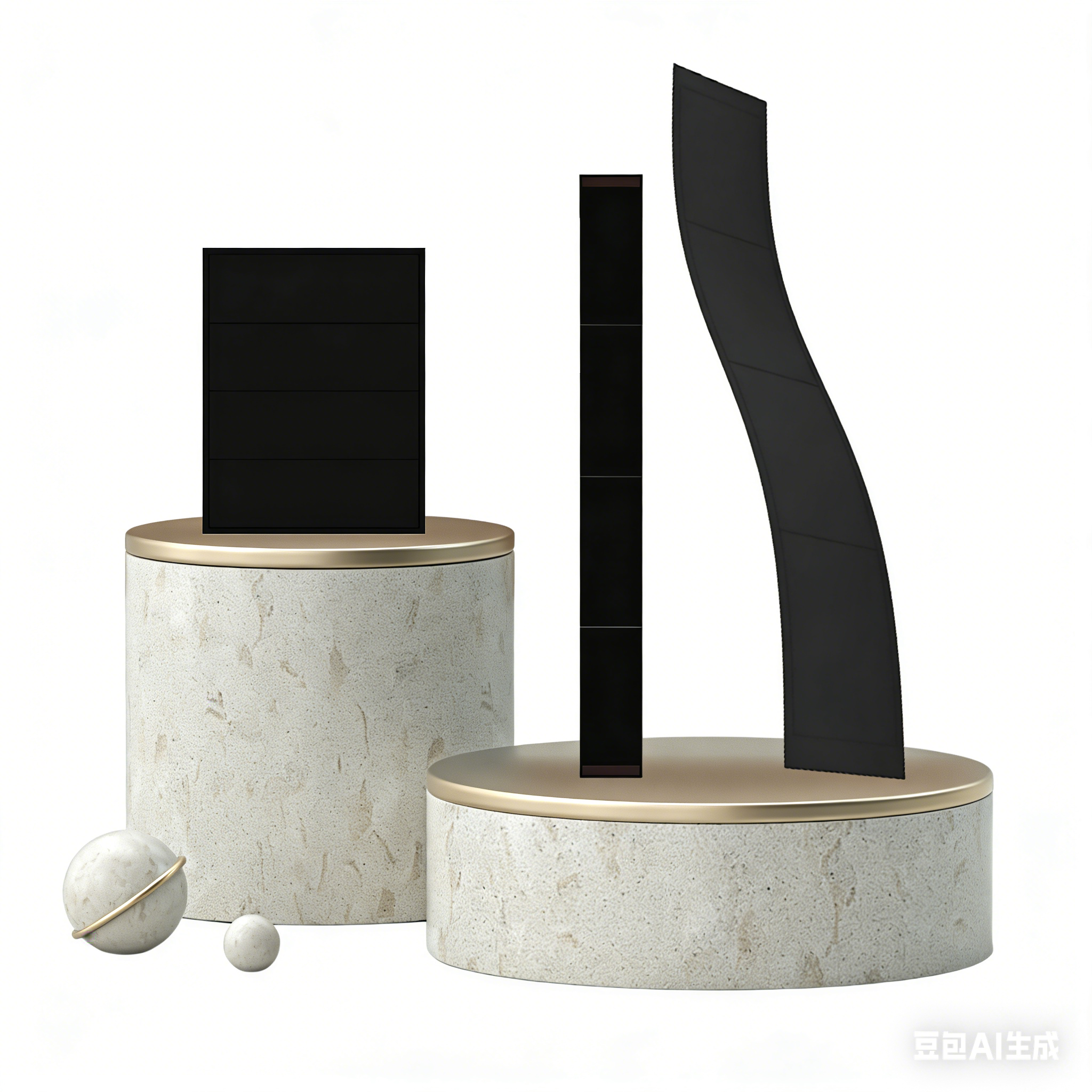
Low-temperature processing enables thin, flexible cells that conform to curved surfaces and integrate easily into consumer electronics.

Excellent optical response in the visible range

Excellent optical response in the visible range

Perovskite materials exhibit strong light absorption across the 400–750 nm spectrum, enabling efficient power generation even under indoor lighting and enhancing energy autonomy for smart devices.

WHY CHOOSE YANHE

Scalable Manufacturing

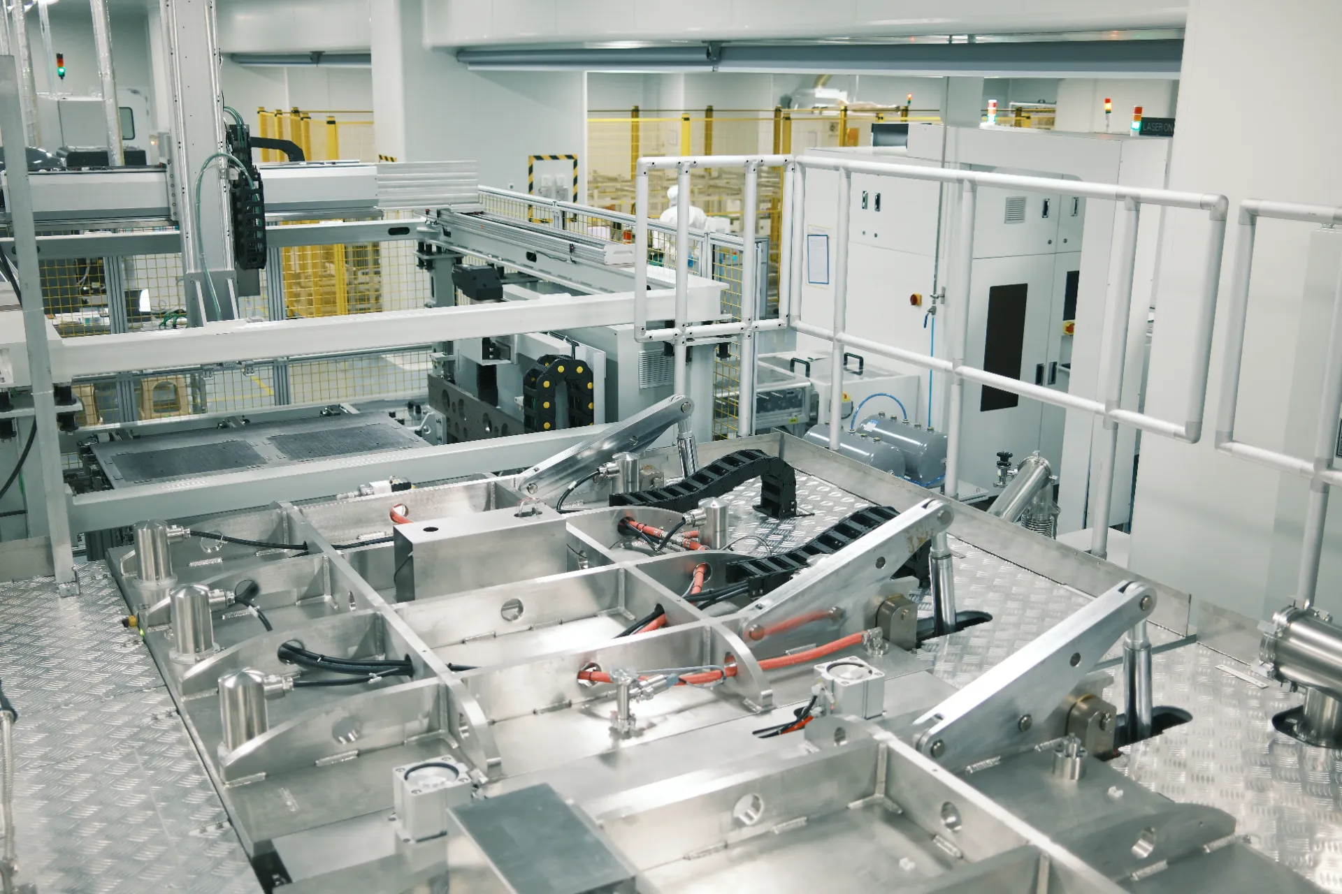
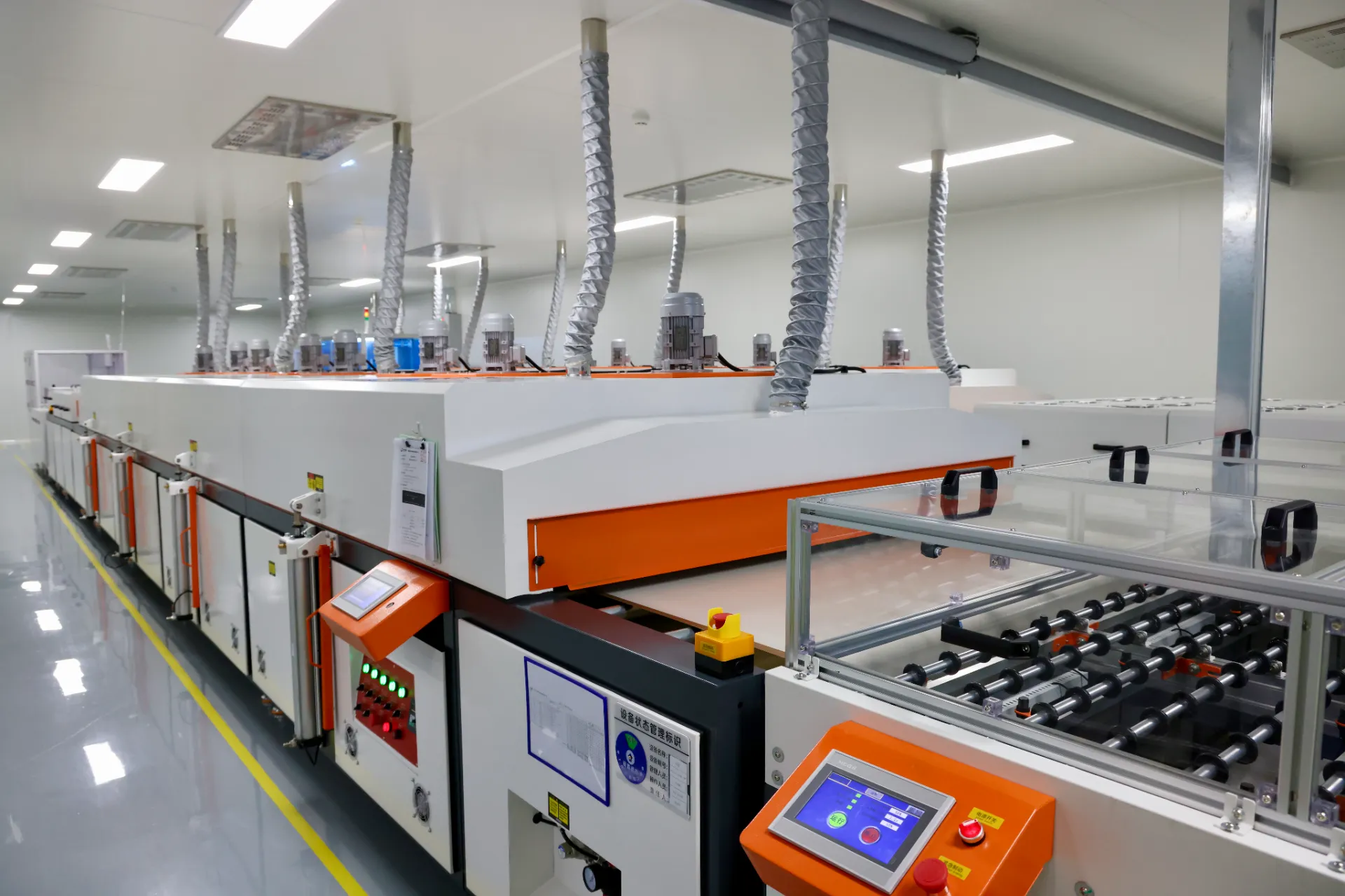
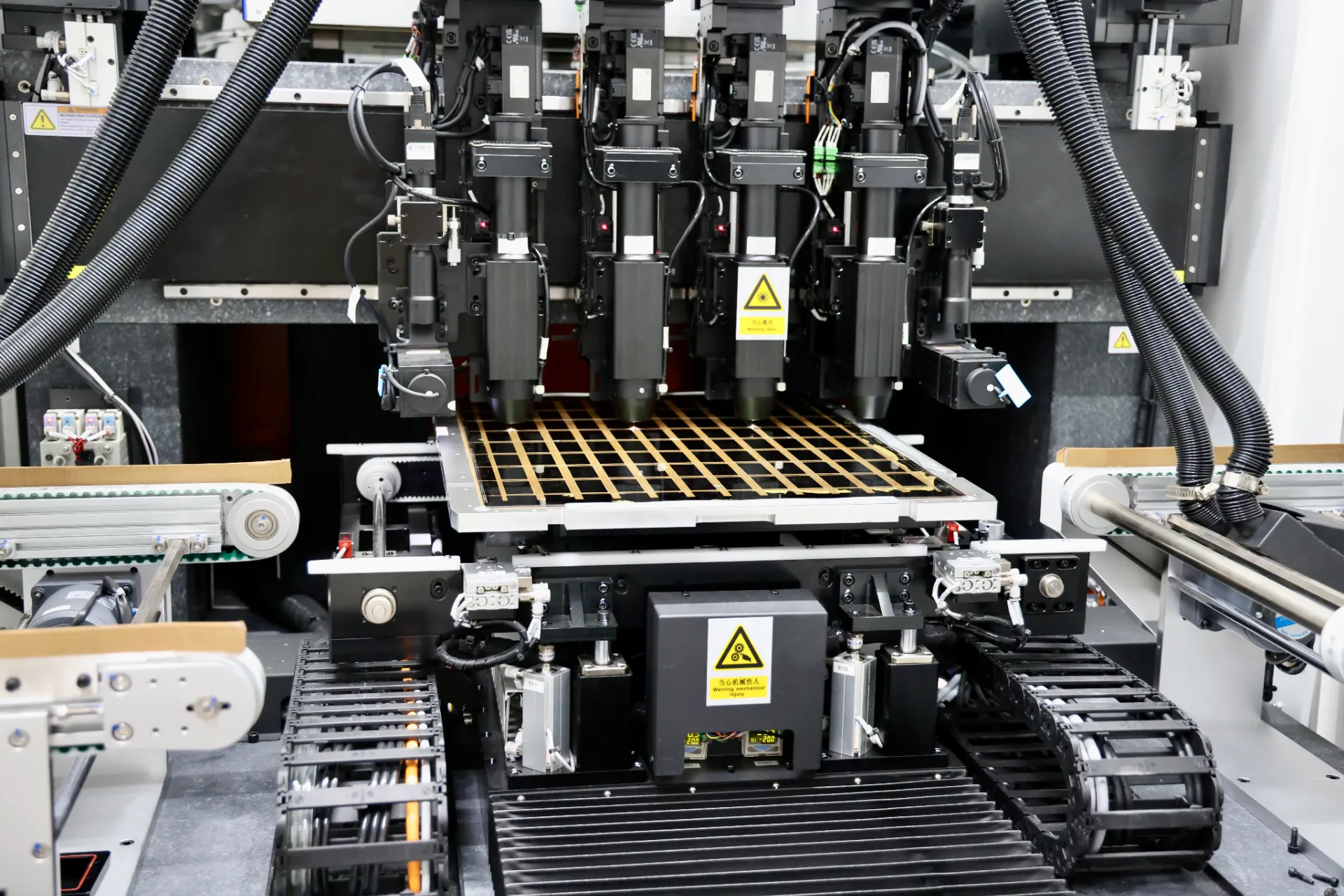
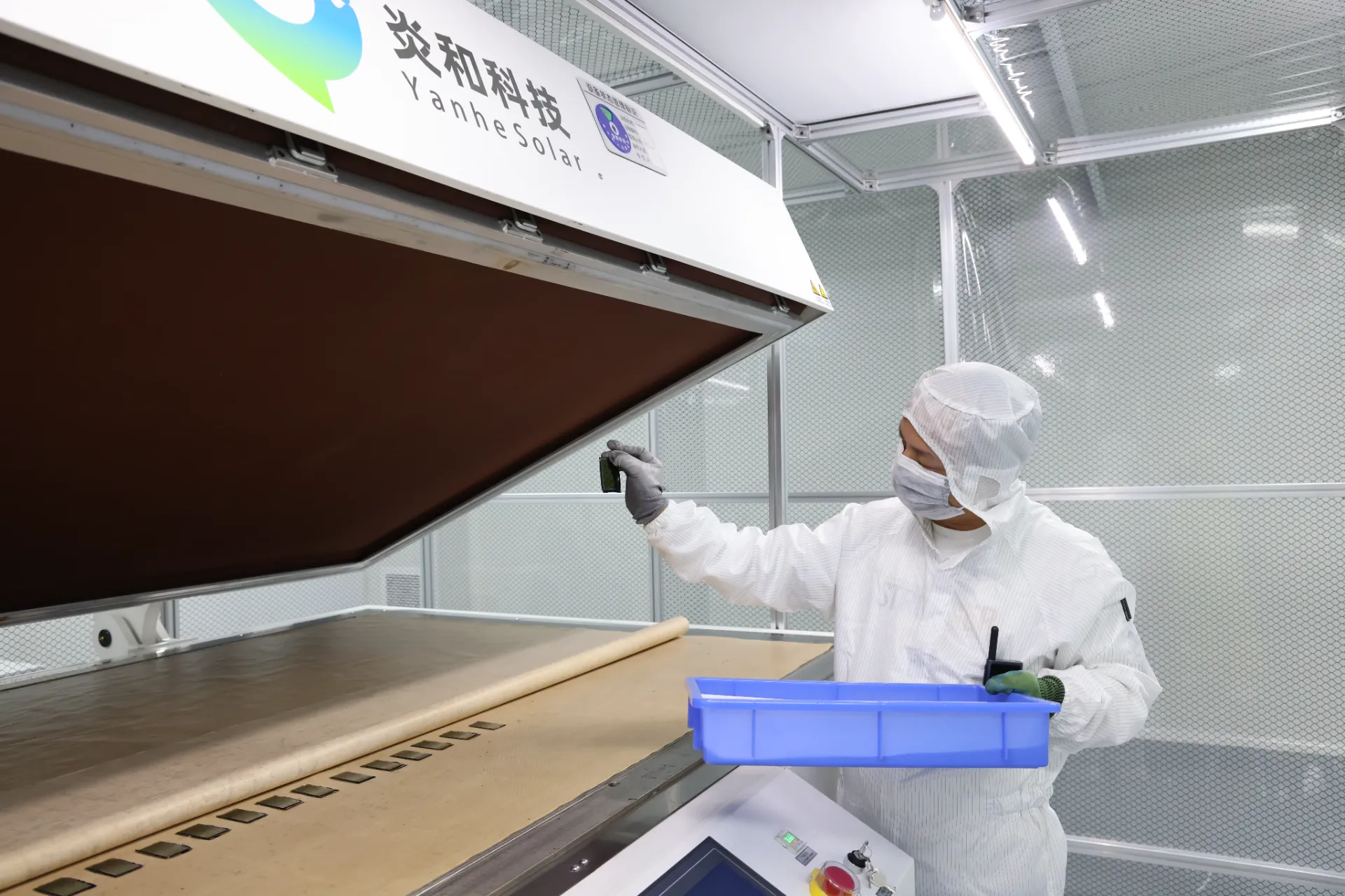
Mass production across diverse form factors, powered by the world's first fully automated consumer perovskite solar cell production line.

Scalable Manufacturing

Cost-Efficient Modules

Improved film uniformity and yield enable lower costs for consumer and flexible electronics.

Cost-Efficient Modules
High-Stability Materials

High-Stability Materials

Quasi-2D perovskites with low ion migration enable longer device lifetimes.

Consumer-Grade Packaging

Consumer-Grade Packaging

Ultra-thin, multifunctional encapsulation ensures durability and sleek design.

Production Level - Mass Producibility

The team possesses strong equipment R&D capabilities and production experience in photovoltaic consumer electronics and other fields, enabling efficient mass production of products in any shape. We own the world's first fully automated production line for consumer-grade perovskite cells

Module Level - Low Cost

Breaking through traditional manufacturing process bottlenecks, significantly improving large-area film uniformity and production yield, reducing costs. The technology has been successfully applied in consumer electronics and flexible device fields

Material Level - High Stability

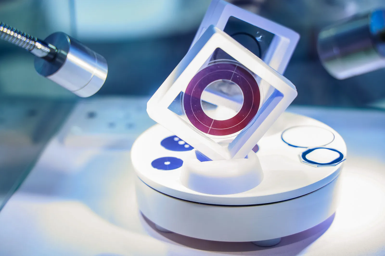
Self-developed high N-value quasi-2D perovskite materials with excellent charge transport performance and extremely low ion migration rate, significantly extending device lifespan and overcoming perovskite stability challenges

Encapsulation Level - Consumer-Grade Aesthetics

Innovative ultra-thin multifunctional encapsulation technology that combines aesthetics with durability, meeting the usage requirements of consumer-grade products